The AI chip race is getting so intense that some of the biggest names in semiconductors and Big Tech are heading back to the classroom.
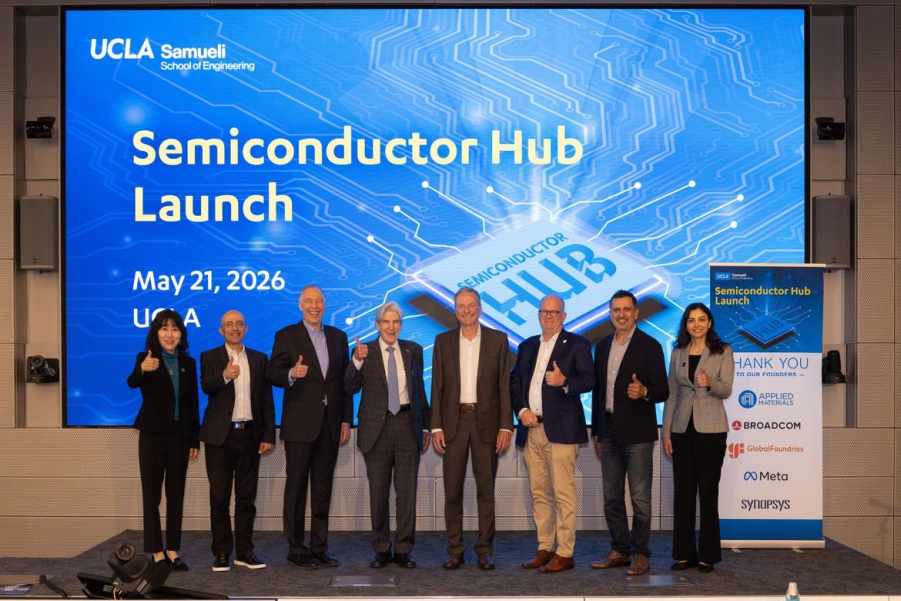
Broadcom, Meta, Applied Materials, GlobalFoundries, and Synopsys are joining forces to launch a $125 million Semiconductor Hub at UCLA to accelerate breakthroughs in next-generation AI chips and train the engineers needed to build them. The new research center will connect students and faculty directly with industry leaders working on chip design, manufacturing, AI infrastructure, and semiconductor software as demand for AI hardware surges worldwide.
The five-year partnership brings together companies spanning nearly every layer of the chip supply chain, from design software and manufacturing tools to chip production and AI infrastructure itself. The goal is to shorten the path between university research and commercial deployment at a time when demand for AI hardware is climbing faster than the industry can comfortably supply it.
UCLA unveils $125M Semiconductor Hub with Broadcom, Meta, and Synopsys to train next-gen AI chip talent
The hub will focus on AI-powered semiconductor technologies, including chip design, manufacturing equipment, software, packaging, and related infrastructure, according to UCLA.
The timing matters.
AI has triggered one of the biggest shifts the semiconductor sector has seen in decades. Companies are racing to build faster, more efficient chips for training and running large AI models, prompting universities, startups, and established chipmakers to collaborate more closely. At the same time, the industry faces growing pressure to rebuild America’s semiconductor workforce after years of dependence on overseas manufacturing and a shortage of specialized engineering talent.
“UCLA is uniquely positioned to bring together expertise across disciplines to push the frontiers of semiconductor innovation and translate that knowledge into scalable solutions,” Frenk said. “The Semiconductor Hub at the UCLA Samueli School of Engineering reflects our commitment to forging partnerships with industry in a field critical to economic vitality and national security.”
Ah-Hyung “Alissa” Park, dean of engineering at UCLA Samueli, said the industry itself is still trying to figure out where semiconductor technology will be a decade from now.
“Nobody — including industry — know[s] what a semiconductor industry [is] going to look like in 10 years,” Park told CNBC. “But can we continue to ask [the] most challenging, difficult questions, and high-risk, high-return kind of questions? That’s what we are hoping to do, because this conversation is happening [in a] very sluggish way.”
UCLA Semiconductor Hub
The initiative will include yearlong internships for doctoral engineering students with participating companies, giving researchers direct access to commercial chip development pipelines and industry mentors.
“The vision for the Semiconductor Hub took shape after a conversation with Henry Samueli, one of the most influential innovators of our time,” said Ah-Hyung “Alissa” Park, the Ronald and Valerie Sugar Dean of Engineering at UCLA Samueli. “Henry cofounded Broadcom while teaching at UCLA, underscoring the school’s strong position to help drive semiconductor innovation for a new era of AI. We are thrilled to partner with our founding member companies to share a bold vision addressing both the opportunities and challenges that will define the next decade and beyond.”
Park said the combination of academic and corporate guidance could create stronger long-term career opportunities for students entering a semiconductor sector that has become central to the AI economy.
“I think understanding how you evolve and grow as an independent researcher and engineer — that’s important,” Park said. “So, having a mentorship from not only faculty members but also industry, I think it will really enrich their growth.”
The launch arrives during a strange moment for the tech industry. AI spending continues to surge across Silicon Valley, driving historic investment into data centers, chips, and infrastructure. Yet many of the same companies funding the AI boom are cutting jobs elsewhere.
Meta, one of the founding partners in the UCLA initiative, is reportedly preparing another round of layoffs this week that could affect roughly 8,000 employees, or about 10% of its workforce.
That contrast is becoming more visible across the tech sector. Companies are reducing headcount in slower-growth divisions and redirecting capital toward AI systems, semiconductor infrastructure, and automation projects considered critical to future competitiveness.
Applied Materials CEO Gary Dickerson framed the UCLA partnership as part of a broader push to tighten cooperation between academia and industry as semiconductor development grows more expensive and technically demanding.
“Strengthening the ties between industry and academia is more important than ever as semiconductor complexity increases and the pace of AI development accelerates,” Dickerson said in a statement. “We look forward to working closely with the Semiconductor Hub partners to bring technology breakthroughs to market faster while inspiring the next generation of engineering talent in the U.S.”